From the development history of spark optical emission spectrometer, it can be seen that the early days of PMT spark optical emission spectrometer, the recent emergence of CCD spark optical emission spectrometer, due to its full spectrum analysis, the characteristics of easy expansion quickly eroded many PMT markets. However, PMT spark optical emission spectrometer have a high market share in some large steel mills or companies with high detection accuracy requirements. The main reason is that there are still some shortcomings in CCD detection. However, COMS is said to have great advantages, high sensitivity, and good detection limit, so that high precision like PMT can be achieved. Such a spark optical emission spectrometer with both CCD and PMT advantages should be very promising.
For spark optical emission spectrometer, most of the CCDs used in optical emission spectrometer are made of SONY. They are civilian products and are inexpensive. They are used on cameras (more than 100 cameras); while CMOS is produced by Hamamatsu, Japan, and the cost is high. A big cut. As for the function, since Hamamatsu made this product, and it is for the spark optical emission spectrometer, it must have its meaning.
As for the online CCD cost is higher than CMOS, it is used in high-end SLR machines, high-end CCD cost is very high, is thousands or even tens of thousands of prices, so developed CMOS ready to replace CCD, this CMOS is relatively high-end The cost of CCD has been saved a lot, but it can replace most of the functions of CCD, so the price of mid-to-high-end SLR has dropped a lot.
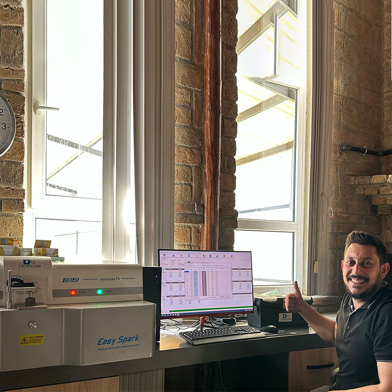
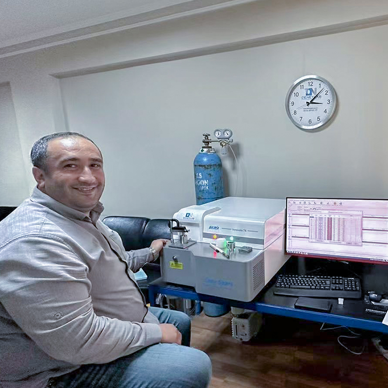
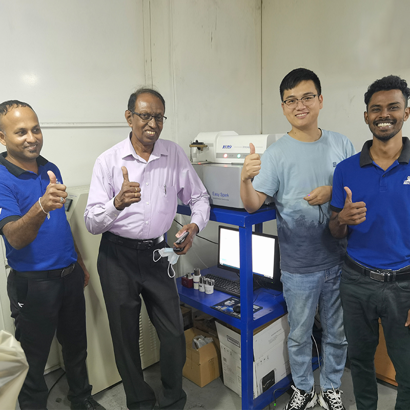
Commercially available instruments have been available a few years ago for spark optical emission spectrometer using CMOS detectors. In order to make the spark optical emission spectrometer better adapt to the analysis of high-purity samples, China's spark optical emission spectrometer industry leads the enterprise--Wuxi Jiebo Instrument Technology Co.,Ltd. is the first to propose the application of scientific research-grade CMOS (complementary oxidized metal semiconductor) as a detector with existing structure and hardware. The idea of combining high-performance spark optical emission spectrometer, and the first release of China's first full-spectrum optical emission spectrometer using CMOS technology - lnnovate T5.

Why CMOS optical emission spectrometer can simultaneously have full spectrum characteristics and ultra low detection limit, mainly due to the following: (1) High sensitivity: Scientific grade CMOS has high for high pixel fill rate of nearly 100%. Spectral imaging system has the sensitivity advantage and good sensitivity. It is applied to optical emission spectrometer. The detection limit of elemental elements of common metal analysis can reach 0.01~10 ppm. (2) Wide spectral range: CMOS optical path structure makes the original continuous spectrum Divided into two sections of spectrum arranged above and below, the effective extended area array sensor accepts the spectrum range and can receive wavelength lines from the deep ultraviolet region to 1000 nm, which can meet the analysis of each element in the metal sample; (3) High impedance: CMOS The integration of the circuit design is higher, the A/D converter is integrated into the chip, and the direct digital signal output greatly reduces the complexity of the peripheral circuit and reduces the power consumption of the whole circuit; the CMOS APS quantum efficiency is relatively high. Due to the new noise cancellation technology, the quality of the output graphics signal is much higher than before, and the readout noise is generally 14 to 100 electrons. Low power consumption, small background and low noise, which greatly improve the repeatability of spectrometer analysis of low content elements; (4) Fast data transmission speed: As can be seen from the internal structure of CMOS, CMOS photodetection and output amplifier are in pixels Internal, so it can read the signal very flexibly, and the CMOS photoelectric sensor can extract the electrical signal while taking out the electrical signal, and can also process the image information of each unit at the same time, so the CMOS data transmission speed is much faster than the CCD charge coupler. . (5) Low cost: Scientific CMOS is also a surface measurement, which can perform full-spectrum scanning and analysis. It does not need to have a tube in a channel like PMT, and the cost is low. The combination of scientific research CMOS and spectrometer is efficient and quality. The combination of the two complement each other. The high-performance, cost-effective CMOS direct reading spectrometer is the product of the progress of the times, the product of market demand, and the inevitable trend of the development of the direct reading spectrometer industry.